A Comprehensive Guide to DIY Home Printed Circuit Boards
Category : |
Sub Category : Posted on 2023-10-30 21:24:53
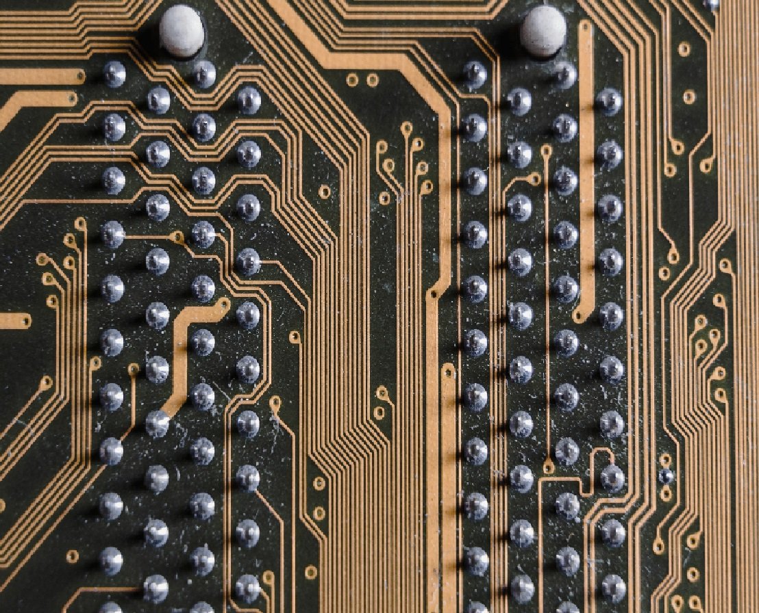
Introduction: Printed Circuit Boards (PCBs) are an essential component of modern electronics, acting as a base for interconnecting electronic components. While there are professional PCB manufacturing services available, many DIY enthusiasts and hobbyists prefer to create their own PCBs at home. In this guide, we will explore the step-by-step process of creating DIY home printed circuit boards, including the necessary materials, techniques, and tips for success. 1. Understanding the Basics of PCB Design: Before diving into the PCB fabrication process, it's important to have a solid understanding of PCB design. Familiarize yourself with the basic concepts, including component placement, routing, and signal integrity. Design software such as Eagle, KiCad, or EasyEDA can help you create your PCB layout efficiently. 2. Gathering the Necessary Materials: To create your own PCB at home, you'll need a few essential materials. These include: - Copper Clad Board: A copper clad board acts as the base material for your PCB. It's a flat board covered with a layer of copper on one or both sides. - Etching Solution: An etching solution, such as ferric chloride or ammonium persulfate, is used to remove unwanted copper from the board during the etching process. - Resist: A resist material such as photoresist or toner transfer paper is used to protect the areas of the PCB where copper traces should remain. - PCB Drill Bits: High-speed drill bits are necessary for drilling holes for component placement on the board. - Soldering Iron and Solder: These will be used to solder the electronic components onto the finished PCB. 3. Transferring the Design onto the PCB: There are various methods to transfer the PCB design onto the copper clad board. The most common methods include: - Toner Transfer Method: This involves printing your PCB design onto a special transfer paper using a laser printer and then transferring the toner onto the copper surface using heat. - Photoresist Method: In this method, a light-sensitive photoresist is applied to the copper surface. The PCB design is then exposed onto the photoresist using a UV light source. 4. Etching the PCB: Once the design is transferred onto the copper surface, it's time to etch the board. Follow the instructions provided with your chosen etching solution carefully. Typically, this involves immersing the board in the etching solution until all unwanted copper is removed, leaving only the desired copper traces intact. 5. Drilling Holes and Finalizing the PCB: After etching, drill holes into the PCB using the appropriate drill bits. These holes will allow for component placement and soldering. Ensure that the hole sizes match the component leads. Finally, clean the PCB to remove any residues from the etching process and make any necessary touch-ups before starting the soldering process. 6. Soldering the Components: With the PCB ready, it's time to solder the electronic components onto the board. Carefully follow the component placement and soldering instructions from your circuit design. Ensure proper solder joints and connections for optimal functionality. Conclusion: Creating your own DIY home printed circuit boards can be a rewarding experience for electronics enthusiasts. By following the steps outlined in this guide and using the appropriate materials and techniques, you can successfully fabricate your own custom PCBs from the comfort of your home. Remember to practice caution and precision throughout the process for the best results. Happy PCB making! For a different angle, consider what the following has to say. http://www.svop.org to Get more information at http://www.mimidate.com


