The Evolution of Electronic Devices: From Registration to Printed Circuit Boards
Category : |
Sub Category : Posted on 2023-10-30 21:24:53
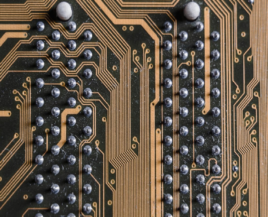
Introduction In today's era of advanced technology and sleek gadgets, it's hard to imagine a world without electronic devices that have become an integral part of our daily lives. From smartphones to laptops, smartwatches to home automation systems, the evolution of electronic devices has been nothing short of remarkable. In this blog post, we will explore the journey of electronic device history from the early days of registration to the advent of printed circuit boards (PCBs). Registration of Electronic Devices Before the widespread use of PCBs, electronic devices relied on a complex network of wires, tubes, and manual connections. The process of manufacturing electronic devices was tedious and time-consuming. Each connection had to be manually soldered and tested, making it an expensive and inefficient process. In the early days, electronic devices were not as small or portable as we know them now. They were bulky and often confined to specific locations such as laboratories or industrial settings. However, with the advancement of technology, engineers and designers began to explore ways to make these devices more compact and user-friendly. Enter the Printed Circuit Boards The introduction of printed circuit boards revolutionized the electronics industry. A printed circuit board, commonly known as a PCB, is a thin board made of non-conductive material like fiberglass, with thin layers of conductive material etched onto it. These conductive paths, also known as traces, replace the need for manual wiring, making the manufacturing process much more efficient. PCBs brought numerous advantages to the electronic device industry. They provided a reliable platform for connecting various electronic components efficiently. The design and fabrication of PCBs allowed for the miniaturization of electronic devices, enabling compactness and portability. Additionally, PCBs improved the reliability and durability of devices, reducing maintenance costs. The PCB manufacturing process involves several steps, starting from the design and layout of the circuit on a computer-aided design (CAD) software. Once the design is finalized, it is transferred onto the PCB through a process called photolithography. This process involves light-sensitive materials and chemical etching to create the desired circuit paths. Afterward, the electronic components are soldered onto the board, and the device is ready for use. Impact on Electronic Device Innovation The advent of printed circuit boards had a significant impact on the innovation and development of electronic devices. With the simplification of the manufacturing process, companies and designers were able to create prototypes and test their ideas more swiftly. This led to the rapid advancement of technology and more affordable electronic devices. Moreover, the introduction of PCBs also paved the way for the mass production of electronic devices, making them accessible to a wider audience. The standardization of circuit board designs and the availability of off-the-shelf components made it easier for companies to manufacture electronic devices in large quantities, reducing costs and increasing market availability. Conclusion The history of electronic devices has come a long way, from the laborious process of manual registration to the innovation of printed circuit boards. PCBs have not only enhanced the functionality and reliability of electronic devices but also played a crucial role in shaping our modern world. As technology continues to advance, we can expect further improvements in the design, manufacturing, and performance of electronic devices, ensuring a bright and exciting future for the world of electronics. For a different angle, consider what the following has to say. http://www.edhr.org


