Exploring the Pros and Cons of Through-Hole Technology in Electronic Products
Category : |
Sub Category : Posted on 2023-10-30 21:24:53
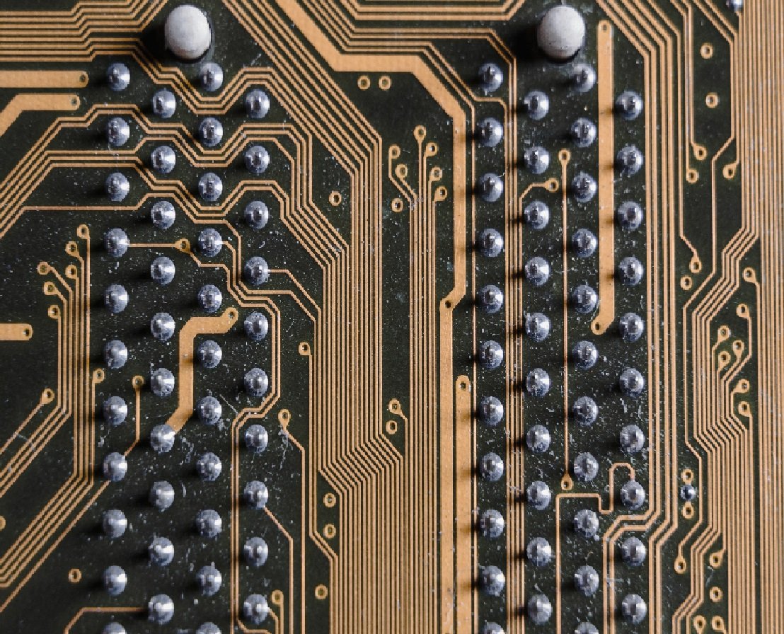
Introduction When it comes to designing and manufacturing electronic products, engineers have a wide array of options to choose from. One such option is through-hole technology, a method that has been in use for decades. In this blog post, we will dive deep into through-hole technology in electronics, exploring its benefits and drawbacks. Understanding through-hole technology Through-hole technology is a method used for mounting components onto a printed circuit board (PCB). In this technique, leads of the components are inserted into pre-drilled holes in the PCB and soldered on the opposite side. This approach offers several advantages over surface-mount technology, which has gained popularity in recent years. Benefits of through-hole technology 1. Durability and reliability: Through-hole components are known for their robustness and ruggedness. They can withstand high temperatures, shocks, and vibrations, making them ideal for applications that require resilience, such as aerospace and defense industries. 2. Mechanical stability: The through-hole method provides excellent mechanical stability, as the components are firmly soldered onto the PCB. This makes them less prone to damage caused by physical stress, ensuring better long-term reliability. 3. Heat dissipation: Through-hole components have larger physical footprints compared to their surface-mount counterparts. This larger size allows for better heat dissipation, making them suitable for high-power applications that generate significant amounts of heat. 4. Repairability: One of the significant advantages of through-hole technology is its repairability. In case a component fails or needs to be replaced, it can be easily desoldered and replaced without causing significant damage to the surrounding circuitry. Drawbacks of through-hole technology 1. Larger PCB footprint: Through-hole components require larger holes and more substantial PCB traces, resulting in larger overall PCB sizes. As a result, through-hole technology is not the best choice for miniaturized and compact devices. 2. Higher manufacturing costs: The process of drilling holes and soldering components in through-hole technology is more labor-intensive and time-consuming than surface-mount technology. This leads to higher manufacturing costs, making it less suitable for budget-sensitive projects. 3. Limited component availability: With the industry's shift towards surface-mount technology, the availability of through-hole components has decreased over time. This limitation can pose challenges when sourcing specific components or when designing new projects that rely on through-hole components. Conclusion Through-hole technology has been a mainstay in electronics manufacturing, offering several advantages over surface-mount technology. Its durability, mechanical stability, heat dissipation capabilities, and repairability make it a viable choice for applications that require reliability and robustness. Despite its drawbacks of larger PCB footprint, higher manufacturing costs, and limited component availability, through-hole technology continues to have its rightful place in the electronics industry. It ultimately comes down to the specific requirements of each project and the tradeoffs involved in choosing the right technology for the job. For a detailed analysis, explore: http://www.wootalyzer.com


