Top Tips and Tricks for Effective PCB Design Software Usage
Category : |
Sub Category : Posted on 2023-10-30 21:24:53
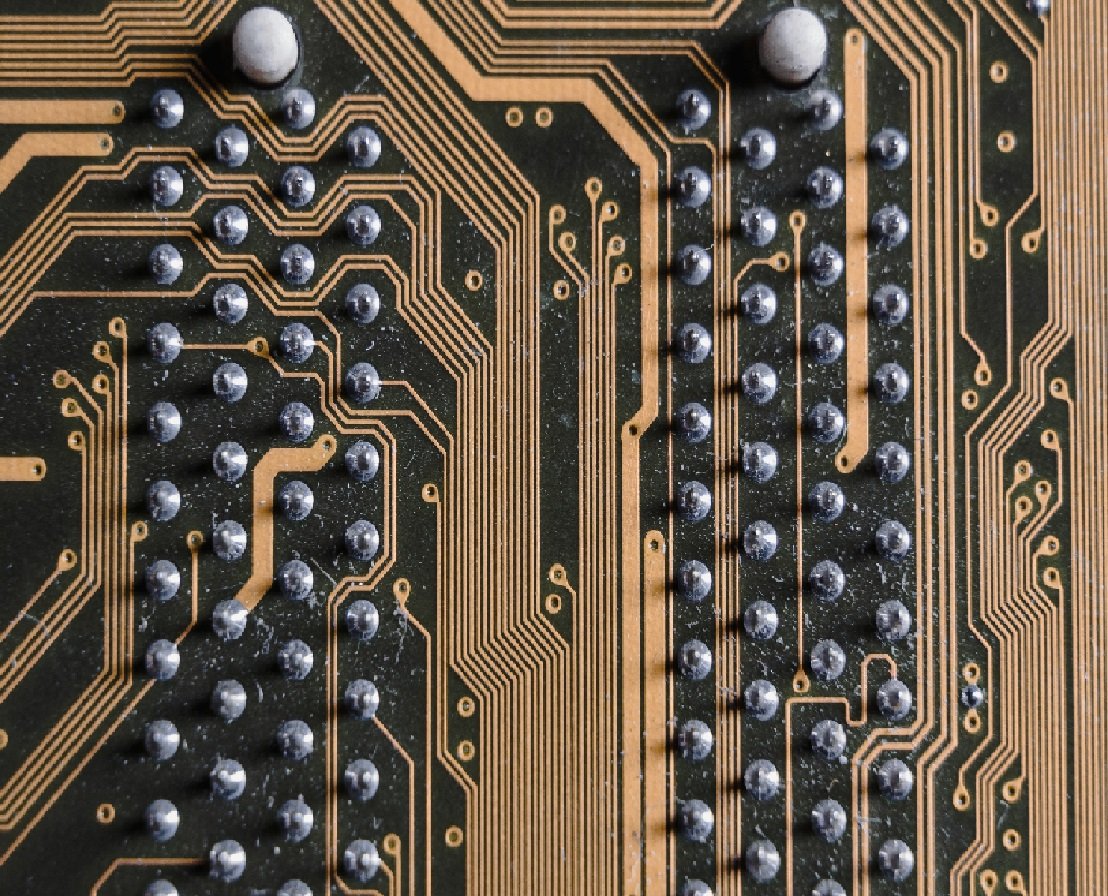
Introduction: PCB design software has revolutionized the way electronic engineers design and develop printed circuit boards (PCBs). These software solutions offer a wide range of features and capabilities that allow the design process to be more efficient and accurate. In this blog post, we will explore some essential tips and tricks to help you maximize your productivity and create high-quality PCB layouts using PCB design software. 1. Familiarize yourself with the software interface: When starting with a new PCB design software, take the time to explore its interface, understand its different menus, toolbars, and shortcuts. Get acquainted with the various tools and functions available, as this will greatly improve your efficiency during the design process. 2. Utilize design rule checks (DRC): Design rule checks are essential for ensuring that your PCB design meets the required specifications and manufacturing constraints. These checks can detect potential issues like clearance violations, incorrect pad sizes, or improperly placed components. By running regular DRC checks, you can prevent costly mistakes and save valuable time. 3. Make use of grid and snap features: To ensure precise component placement and accurate routing, leverage the grid and snap features offered by the PCB design software. Adjusting the grid spacing and snap settings will allow you to align components and route traces with greater accuracy, resulting in a higher quality PCB layout. 4. Create and utilize design templates: Design templates provide a starting point that can significantly speed up your design process, especially when working on PCBs with similar layouts or designs. By creating and utilizing design templates, you can utilize pre-defined settings, layers, and component placements, saving time and effort. 5. Use libraries and component footprints: Most PCB design software solutions offer extensive libraries with pre-built components and footprints. Take advantage of these libraries to quickly add commonly used components to your design. Additionally, make sure to customize and create your own component footprints when necessary, ensuring accurate representation and compatibility with your specific PCB design requirements. 6. Utilize design hierarchy and hierarchical design: When working on complex PCB designs, using design hierarchy allows you to divide your layout into smaller, manageable sections. Hierarchical design enables you to focus on specific areas while maintaining a clear overview of the entire project. This approach greatly simplifies design updates and makes collaboration with team members more efficient. 7. Experiment with design constraints and rules: PCB design software allows you to define various rules and constraints to guide your design process. Take the time to experiment with constraint settings to optimize your design for factors such as signal integrity, trace lengths, or power distribution. Understanding and utilizing these constraints will help you create a more robust and reliable PCB layout. 8. Use autorouting with caution: While autorouting features can be helpful for simplifying and speeding up the routing process, they should be used with caution. These features can sometimes create suboptimal results, leading to issues such as increased trace length mismatch or inefficient use of PCB real estate. It is recommended to manually route critical and sensitive traces, while utilizing autorouting for simpler connections. Conclusion: By following these tips and tricks, you can enhance your proficiency in using PCB design software and streamline your design process effectively. Maximizing your familiarity with the software interface, leveraging design rule checks, using design templates and libraries, employing design hierarchy, and experimenting with constraints will help you create high-quality PCB layouts efficiently. Remember, practice makes perfect, so don't hesitate to explore additional features and techniques that suit your specific design requirements. Happy PCB designing!


